The semiconductor industry is evolving at an unprecedented pace, driven by the demand for cutting-edge electronics in fields such as artificial intelligence (AI), 5G networks, electric vehicles (EVs), industrial automation, consumer and medical electronics. To stay ahead, designers are continually pushing the limits of chip design, striving for smaller, more energy-efficient, and higher-performing solutions. In industries such as EVs, AI-powered data centers, medical devices, and manufacturing, even a slight improvement in chip performance can translate into substantial competitive advantages.
Power, Performance, and Area
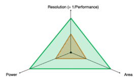
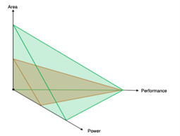
As technology advances, the demand for more compact and powerful semiconductor solutions grows. Designers must balance several critical factors, including performance, power consumption, and size, known collectively as the PPA (Power, Performance, and Area) indicators. This metric plays a pivotal role in selecting semiconductor components and process technologies to meet evolving market demands. As a pure number, the PPA Figure-of-Merit (FoM) is normally expressed as: PPAFOM=Performance/(Area x Power)
However, the PPA metric may also be expressed graphically as a 2D triangle or a 3D pyramid.
Low power consumption, high performance (or smallest resolution, when expressed in mV/LSB) and reduced silicon area are often used to characterize the competitiveness of a circuit and / or process technology. These three variables generally create a trade-off during schematic design with an improvement in one often negatively impacting another. The question is, with PPA as figure of merit, which integral improvement in analog circuits can be reached by moving to a next generation process technology?
Deep Dive into PPA: TND6465 - High Performance, Precision Analog Capability Enabled by the Treo Platform
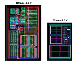
The Treo Platform’s Technological Leap: 65nm BCD vs. 180nm CMOS
To address these challenges, onsemi introduced the Treo Platform, a cutting-edge semiconductor technology platform designed to support next-generation analog and mixed-signal products. Treo is built on BCD (Bipolar-CMOS-DMOS) technology, and unlike existing BCD platforms, Treo offers an industry-leading voltage range of 1V to 90V, enabling exceptional integration, reduced power consumption, and unparalleled efficiency. By leveraging 65nm process technology, onsemi significantly enhanced the capabilities of semiconductor design compared to older 180nm CMOS technologies.
There are a number of key benefits of Treo’s 65nm BCD technology including:
- Power Efficiency: The reduced gate oxide thickness enables lower supply voltages (2.5V vs. 3.3V or 5.0V), which can result in power savings of up to 25% or 50%. Actual power reductions may vary and can exceed this figure due to decreased current consumption.
- Size Reduction: Shrinking from 180nm to 65nm process technology allows for a significant reduction in low-voltage analog circuit area.
- Performance Gains: With improved transistor matching and smaller geometries, Treo-based solutions achieve higher precision and greater bandwidth for the same power budget.
- Seamless High-Voltage Integration: Treo enables high-voltage components to be embedded within the chip itself, eliminating the need for external power modules and simplifying design complexity.
Case Study: Treo’s Advantage in an Operational Amplifier Circuit
To demonstrate the Treo Platform’s advantages, onsemi conducted a direct comparison between a two-stage Miller operational amplifier designed in 180nm CMOS and one ported to Treo’s 65nm BCD platform.
The porting was conducted carefully to ensure equal performance in terms of offset, bandwidth, relative input common mode range, etc. After manufacturing, both circuits were characterized to identify the improvements made by porting to the Treo process.
The results showed clearly the significant benefits of designs developed in the Treo platform:
- Power Consumption: Reduced by a factor of 2.2x, meaning the new design consumes less than half the power of the older one.
- Chip Area: Reduced by 43.1%, translating into a 2.32x improvement in silicon usage.
- Overall PPA Figure-of-Merit (FoM): The Treo-based design outperformed the 180nm version by a factor of 5.1x.
These enhancements not only improve efficiency but also allow designers to integrate more functionality and performance into smaller devices, making next-generation semiconductor products more competitive and cost-effective.
Manufacturing Excellence
While technological advancements in chip design are essential, a strong manufacturing backbone is equally critical. To ensure consistent supply, onsemi invested in a state-of-the-art semiconductor fabrication facility in East Fishkill, NY. Opened in 2023, this fab plays a key role in producing Treo-based semiconductor solutions using 300mm wafer technology.
By establishing a domestic production facility, onsemi enhances supply chain reliability and reduces dependency on overseas manufacturing. This is particularly crucial in light of global semiconductor shortages and geopolitical uncertainties that have disrupted supply chains in recent years.
Summary
The semiconductor industry stands at a pivotal moment, with increasing demand for higher efficiency, smaller form factors, and improved performance. onsemi’s Treo Platform, with its advanced 65nm BCD technology, represents a significant leap forward, offering substantial benefits over traditional analog and mixed-signal solutions.
With the support of a resilient supply chain and cutting-edge manufacturing, the Treo Platform is set to redefine the semiconductor landscape, providing the power-efficient and high-performance chips that will drive the next wave of technological innovation. Whether in AI, automotive, medical, or industrial applications, Treo is paving the way for a smarter, more connected world.
Additional Resources
TND6465 - High Performance, Precision Analog Capability Enabled by the Treo Platform
TND6464 - High Temperature Analog and Mixed‐Signal Solutions Enabled by the Treo Platform
T30HM1TS2500
Treo Platform Technology | onsemi